Dean's Message
Esteemed visitors, welcome to the Department of Electronics and Communication Engineering at KIET.
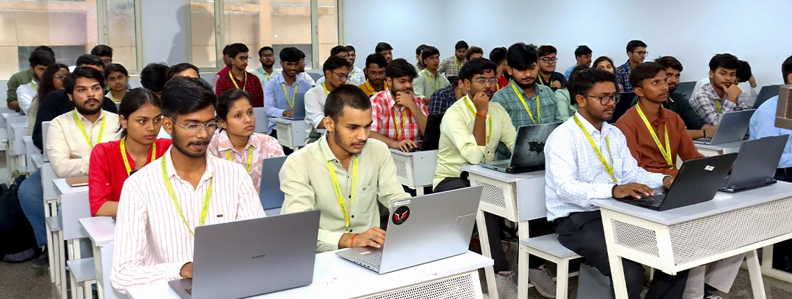
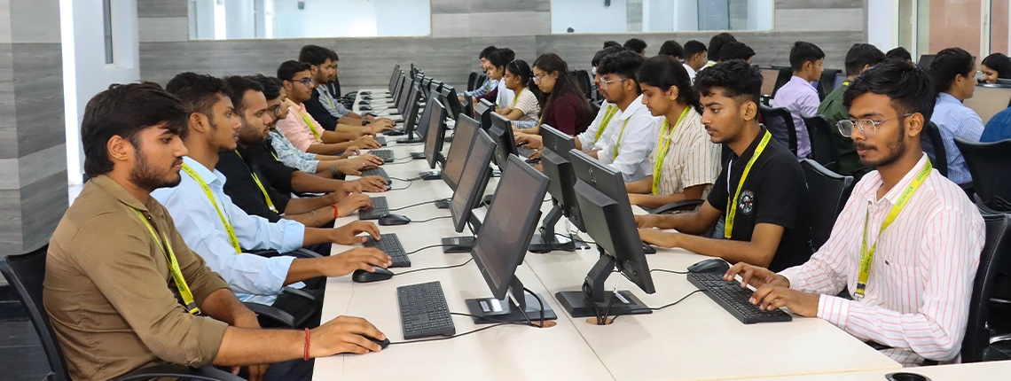
In today’s rapidly evolving technological landscape, Electronics and Communication Engineering remain a driving force, propelling innovation across countless sectors. Established in 1998, our department has a rich history of academic excellence and impactful research. We proudly offer two undergraduate programs: Electronics & Communication Engineering (with an intake of 180 students) and Electronics & Communication Engineering – VLSI Design and Technology (with an intake of 30 students). Here at KIET, we are dedicated to providing a transformative educational experience. Our curriculum is meticulously crafted to provide a robust foundation in core electronics principles, while simultaneously offering avenues for specialization in cutting-edge domains such as VLSI Design, Embedded Systems, Signal Processing, System Engineering and Wireless Communication Systems. We place a strong emphasis on hands-on learning, utilizing state-of-the-art laboratories, design projects, and collaborations with industry partners, ensuring that our graduates are exceptionally well-prepared to address real-world challenges.
We cultivate a vibrant learning environment that fosters intellectual curiosity, critical thinking, and collaborative problem-solving. Our dedicated faculty members are not only leading experts in their fields but also passionate educators committed to mentoring and guiding our students towards success. We strongly encourage research and innovation, providing ample opportunities for students to participate in cutting-edge research projects alongside our faculty. The department actively organizes national and international events, including conferences, short-term courses, summer schools, and workshops. Our department is committed to producing high-quality publications in esteemed national and international journals and conferences. In recent years, we have established a strong track record of securing design and product patents.
As Dean of the Department, I am immensely proud of our students, faculty, and alumni, who are making significant contributions to the advancement of electronics engineering and shaping the future of technology. I invite you to explore our website and discover more about our programs, research endeavors, and the exciting opportunities that await you at the Department of Electronics and Communication Engineering. We believe in Alan Kay’s powerful statement: “The best way to predict the future is to invent it.” This belief fuels our dedication to groundbreaking research and transformative education in Electronics and Communication Engineering.
- Prof. (Dr.) Vibhav Kumar Sachan